
How to reduce hot spots
Among the many concerns for designing a 90-200A point-of-load (POL) regulator circuit is the concentration of heat or hot spots, especially when the circuit is intended to fit on a small PCB area, as Afshin Odabaee of Linear Technology explains.
Unresolved, a hot spot degrades reliability by exerting thermal stress on components such as the DC/DC IC or the inductor speeding, ageing and finally reaching failure. Thermal relief methods such as faster air flow and larger heat sinks tend to alleviate the problem but add to the solution cost and are wishful remedies; the inherent cause of the problem, an inferior design or careless selection of components, are ignored. A reliable high power POL distributes heat evenly through its top surface to the air and bottom to the PCB. Advanced product packaging techniques, attentive circuit design and careful choice of components can guarantee a solution that eliminates heat concentration and is reasonably small.
Scaling power
Scaling power refers to the ability to increase power delivered to a load by adding and current sharing several blocks of DC/DC regulator circuits. In contrast to one large high power regulator, blocks of smaller power regulators offer layout flexibility as they can be arranged to occupy odd spaces on a PCB. The key point is precision current sharing. The precision allows each block to share an equal fraction of the total output power distributing the heat evenly among each block of regulators. This allows for easier thermal management and cheaper provisions of removing heat from a high power POL circuit.
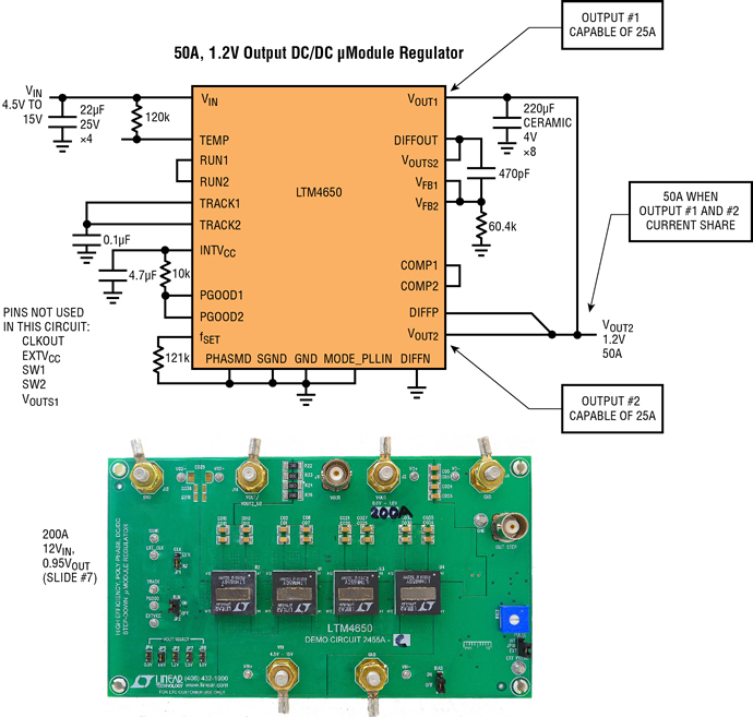
Above: Figure 1: LTM4650 Diagram and 200A Board with four LTM4650s in Current Share
A current mode architecture DC/DC regulator measures the output current to the load on each cycle of delivering the current. With precision measurement and control, and matching this precision between circuits (i.e. blocks), one can achieve a uniform heat dissipation among the circuits.
The LTM4650 is a dual output 25A each µModule (power module) regulator or single output 50A when the outputs are current shared. Two LTM4650 µModule regulators can deliver up to 100A to a load. Four devices in parallel provide as much as 200A. Designed with a current mode architecture DC/DC regulator, the LTM4650 includes inductors, power MOSFETs and the supporting circuitry, and the circuit is housed in a 16x16x4.95mm BGA package.
Embedded heatsinks
In addition to accurate current sharing, the LTM4650 package includes an integrated heatsink which assists in removing heat from the component inside the package to the top of the package where, with the aid of air flow or a heatsink, heat is quickly and smoothly dispersed. A portion of the heat generated in the LTM4650 is also conducted by its multi-layer substrate to the surface of the PCB – as shown in Figure 1.
A current mode architecture DC/DC regulator measures the output current to the load on each cycle of delivering the current. With precision measurement and control, and matching this precision between circuits (i.e. blocks), one can achieve a uniform heat dissipation among the circuits.
The devil’s in the detail
A methodical and proven approach presented here does simplify assigning and managing blocks of power in a system with complex multi-voltage rail requirements. This is the big picture and necessary for a start. However, what about the more refined intricate details? What other power related subjects should a system designer note ahead of time to avoid debugging, spinning the board, or at worst starting over? Here are a series of brief discussions on a few of these ‘other’ subjects that are sure to occupy the time of an engineering team sooner or later.
Any load such as a GPU, FPGA or a processor that is computing or processing bits of data that is subject to randomly high data traffic will require a surge of current which quickly disrupts its steady state power consumption. This transient in current (or power) consumption affects the output voltage of the DC/DC regulator responsible for powering and regulating the voltage of the load. The output voltage of the regulator droops as the regulator fights to supply the load current that is required by the core of the FPGA, for example, while regulating the core voltage. If the regulator is unable to keep up with the regulation while supplying the load current, then there is a problem with a few ideas to ponder a solution:
- Can the loop response of the regulator be compensated? (Playing with the phase margin and bandwidth of the regulators feedback loop).
- Is a more powerful regulator circuit needed?
- Can the addition of more output capacitors (more capacitance) remedy the problem (capacitors can hold charge and help the regulator during load transients)?
Addressing the above list is time consuming - #2 and #3 will also affect a solution cost and size. Aside from being a seasoned analogue and power designer who can prevent headaches early in the design process, there are respected power supply design tools that can assist anyone, even a less experienced system engineer. The existence of an example of a working solution as in a development board for FPGAs and the supporting engineering materials constantly prove their worth by reducing time that is wasted on assessing performance of power management such as in optimising the transient response and minimising a requirement on the number of capacitors.
Sequencing and tracking
More than nine voltage rails in a system and there is inevitably the question of what is the right order. The reverse is also true during the shutdown of a system. The reason is sequential timing between different digital segments of a system each tasked to perform a job that may depend on the status and ‘health’ of another segment. For example, should the core voltage be in regulation first then the I/O starts, then the start of the transceivers? How does one assure that one segment accidentally does not start too early or too late and lock-up the system from powering up?
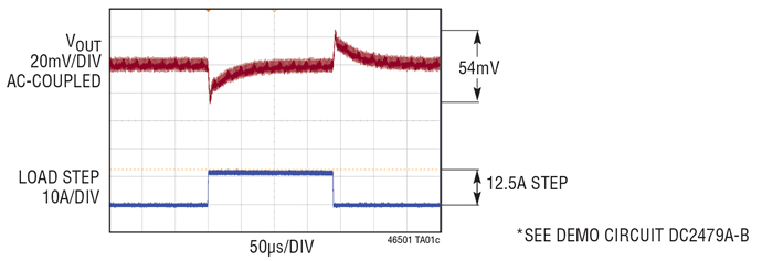
Above: Figure 2: only six 220µF ceramic capacitors for 50A at 1V output; precision ±3% output regulation at transient load step of 25% (LTM4650-1B, demo circuit DC2479A-B)
The sequencing of power-up is recommended by digital chip suppliers such as Xilinx, Intel (Altera), NXP (Freescale) and others. So, this information is known to a system engineer. Then how does one enforce a proper sequencing of power for multiple voltage rails?
This task is relatively simple and most DC/ DC regulators have this function sometimes referred to tracking a voltage. However, as mentioned here, having the function is important but knowing how to set-up the sequence early in the design and simulate it is more important. It saves re-tracing PCB layouts or swapping capacitors and resistors later to fix the power up and down timing of the regulators. Do this exercise early on and be able to power-up a complex multi-rail system the first time.
Scaling power
Every system engineer chooses the spot on the correct power supply point-of-load regulator the first time. This is a myth, of course. For the 90% who at some point during prototyping realise that the regulator is unmatched with the load and feature requirements of the system, this realisation is frustrating. To avoid the agony, most over-design. Or to no fault of the designer, the load’s (FPGA, ASIC, etc.) power consumption is under reported. A 10A load is suddenly in need of 30A due to many factors such as the number of transceivers in use, faster timing, flow of firmware and algorithms, etc. Is there a way to start mapping the power management, choose the part numbers and do the layout while being assured that if power requirement changes, the change in design of power circuit is simple or at least not overwhelming?
Yes, there is this concept of scaling power up or down by adding or removing blocks of regulators. These blocks are also pin-compatible, so the layout can be a matter of copying and pasting the same footprint and same part number or device. For example, a power block (or power module) that is capable of delivering 30A per device can have five of them current sharing to deliver 150A (5x30A) to a 1V load. The key is to make sure that these power blocks can accurately current share so that no one device is over or underused. An overused device will experience higher temperature rise, possible hot spots and may reach its end of life sooner due to higher thermal stress.
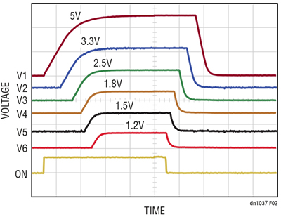
Above: Figure 3: an example of sequencing or tracking 6 voltage rail: 5V rail starts-up and regulates first, 1.2V is last
Pin compatibility is also key because once the layout and pin routing of the device is confirmed, its simply repeating it. To ease the prototyping process and using the earlier example of 150A regulator of 30A per block, a designer can start with all five layouts, populate them and build the board. If board characterisation confirms that a lower current of 115A is sufficient, then instead of five devices, remove one device for 120A and continue with the prototyping.
Or, if you’re starting with 110A with four devices in mind but want to play it safe, then layout a fifth socket but leave it empty and start testing the board. If later during the board evaluation 120A is needed when the board is at its full usage, then simply assemble the fifth power block onto the empty spot without changing the layout and delaying the progress. Move on by focusing on the digital segments of the board where the critical functions are.
Product Spotlight
APV1111GVY
Panasonic

Panasonic PhotoMOS® Photovoltaic MOSFET High-Power Drivers
| SKU: | |
|---|---|
| Stock: | 3490 |
| Cost: | $3.95 |
