It is intended to be used to transfer data between stacked die, or across an array of die on a silicon interposer.
“The steady rise in the number of applications that require high-performance computing creates a demand for new hardware-plus-software communications solutions that improve both performance and energy consumption,” said Leti strategic marketing manager Denis Dutoit. “This technology brick makes it possible to transfer data between processors via a network-on-chip delivering more powerful, energy-efficient computing.”
The aim of this 3D integration project is to provide a high-performance computing block without the high cost (through extremely low yield) that would come from making one enormous 28nm chip, or the high power consumption that would come from linking multiple smaller 28nm chips through a conventional PCB.
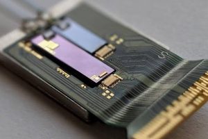
The 3D circuit, currently in foundry, combines a series of identical 28nm die (which Leti calls ‘chiplets’) fabricated on a FDSOI (fully-depleted silicon-on-insulator) process, mounted on an active silicon interposer made on a 65nm CMOS process.
In effect, multiple small high-density processing die – the chiplets – are mounted on a large lower-density communication die.
“The active interposer embeds several lower-cost functions, such as communication through the NoC and system I/Os, power conversion, design for testability and integrated passive components,” said Leti.
Through-silicon vias (TSVs), 1,980 of them, allow the network running on the interposer to reach into the chiplets.
A demonstration of a homogeneous 3D circuit made from regular tiles assembled using a 4 x 4 x 2 network-on-chip has delivered data at 326MFlit/s for an energy consumption of 0.66pJ/bit, according to Leti.
“The chip requires 20 times less energy for data transmission than chips placed on an electronic circuit board,” it said. “This intellectual property is compatible with standard remote direct-memory-access-type software used for data transmission and has likely industrial uses in virtual-server migration applications.”
This article describes other aspects of the same silicon-on-silicon-interposer multi-core processor, which was also discussed at ISSCC this year. “The demo [see photo] was a success, with very good chip-to-chip data transmission speeds-in the hundreds of Mbits/s, for a chip measuring just 40 µm x 40 µm,” said Leti at the time. “Even better, the chip needs 20 times less energy for data transmission than chips placed on an electronic circuit board. This new IP is compatible with standard remote direct memory access-type software used for data transmission and could be of interest to industrial partners for virtual-server migration applications.”