VCSEL Quasi-Array Of Four Devices Outputs 210W At 110A

China’s Changchun Institute of Optics, Fine Mechanics and Physics has developed a module containing four vertical-cavity surface-emitting lasers (VCSELs) capable of emitting 210W at 110A current injection in short-pulse operation [Jianwei Zhang, Jpn. J. Appl. Phys., vol53, p070303, 2014]. The researchers comment: “To the best of our knowledge, this is the highest value reported for a VCSEL module consisting of single emitters.”
The researchers quote comparisons of 92W from a single VCSEL and 123W from an emitter array containing 16 devices.
High-power-output laser diodes find application in laser fusion welding, medical treatment, car-sensing, and laser ranging. VCSELs are attractive for such applications due to good production yields and high reliability in short-pulse operation. The structure suffers less from self-heating that can degrade performance of the active region. Also, the VCSEL architecture does not suffer from the catastrophic optical damage (COD) seen in edge-emitting devices.
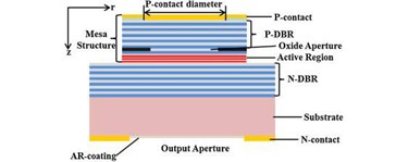
The VCSEL structure (Figure 1) was grown using metal-organic chemical vapor deposition (MOCVD) on n-type gallium arsenide (n-GaAs) substrate. The multiple quantum well (MQW) active region consisted of three 8nm In0.2Ga0.8As wells emitting at 980nm. Distributed Bragg reflectors (DBRs) for such devices typically consist of alternate layers of AlGaAs (or even AlAs) and GaAs.
The mesa etching was carried out using inductively coupled plasma. The oxide current aperture was created using nitrogen gas bubbled through water at 90 °C and delivered to the VCSEL structure at 420°C. The device structure included a 30nm Al0.98Ga0.02As layer above the active region to allow for the selective oxidation.
A plasma-enhanced chemical vapor deposition (PECVD) silicon dioxide insulation layer on the mesa was etched to give a window for the gold p-contact electrode. The bottom of the substrate was coated with an anti-reflection layer for the emission window and gold was used for the n-contact electrode. The devices were cleaved and packaged in TO mountings.
The researchers carried out simulations to find the optimum diameters for the oxide aperture and p-contact. As a result, devices with 200μm, 300μm and 400μm oxide apertures were produced with 160μm, 240μm, and 320μm p-contacts, respectively. The 200μm/160μm device showed the most uniform emission profile, with the larger-diameter devices increasingly suffering the effects of current crowding at the edge of the aperture.
With 100μs quasi continuous wave (QCW) 100 Hz pulsed operation the devices suffered from self-heating effects, particularly the smaller-diameter device. In this mode, the 300μm oxide aperture device had the best maximum output power of 3W. The severe current crowding of the 400μm aperture device reduced its efficiency compared with the 300μm device, although its maximum output exceeded that of the 200μm device.
With short 30ns 5kHz pulses, ‘thermal rollover’ was not observed in any of the devices. The power ordering was the same as for QCW operation. The poor performance of the 200μm device was attributed to carrier leakage at the higher current density relative to the other devices. Such leakage is a more serious problem with very short pulses where carriers injected at a high level into the active region don’t have time to recombine and emit light. The researchers estimate that the current density in the active region of the 200μm device is ten times that of the other VCSELs at the same injection current.
The 400μm device suffered from non-uniformity of the current distribution across the diameter.
The 300μm VCSEL had an external efficiency of 0.62W/A, which is comparable to the reported performance of 5-QW devices. “Moreover, the maximum power of 62W is achieved, which was higher than the record power of proton-implanted single emitters and arrays,” the researchers add.
The researchers also developed a ‘quasi-array’ module (Figure 2) containing four 300μm/240μm oxide aperture/p-contact VCSELs as an alternative to monolithic VCSEL arrays. Problems with monolithic arrays include high operation current, and electrical and thermal crosstalk.
The gold interconnections were designed to be as short as possible to ensure a good short-pulse response of the module. The devices were connected in series. An aluminium nitride (AlN) plate was used as the submount due to the material’s high thermal conductivity. The module was packaged into a TO-39 holder.
In short-pulse operation, the module’s light output was 210W at 110A current input. The performance was limited by the capability of the power supply. This performance is somewhat less than 4x62W = 248W, which the researchers suggest could be due to inductance and capacitance current losses.
The emission wavelength at 110A was 980.5nm with full-width at half-maximum (FWHM) of 1nm. The far-field emission pattern was broad, with a FWHM divergence angle of more than 40°. While this is not desired for applications, the researchers suggest it could be handled with the use of collimating micro-lenses and field lenses.
Source: VCSEL
